


Producing the next generation of semiconductors is, however, becoming increasingly complex. The world’s largest supplier of semiconductor manufacturing equipment, Applied Materials, is set to play a pivotal role in this going forward. We explore the company’s unique differentiators and strong prospects, while unpacking the complexities of the semiconductor value chain and growing challenges in manufacturing.
The building blocks of the digital age
Growth in the semiconductor market will be largely propelled by surging demand in three key areas: AI, the automotive sector and the Internet of Things (IoT).
Within AI, the latest large language models require massive computing power, necessitating more powerful and efficient chips. In the automotive space, modern vehicles now rely on dozens of chips, which is set to increase as the industry shifts toward electric vehicles and autonomous driving. IoT is another major frontier, with billions of sensors and connected devices expected to come on line in the near future.
However, as chipmakers attempt to squeeze more computing power into ever decreasing dimensions, they encounter serious physical limitations. Smaller nodes1 require new manufacturing techniques and materials to maintain energy efficiency and increase performance. Semiconductor equipment suppliers such as Applied Materials, are crucial in this context.
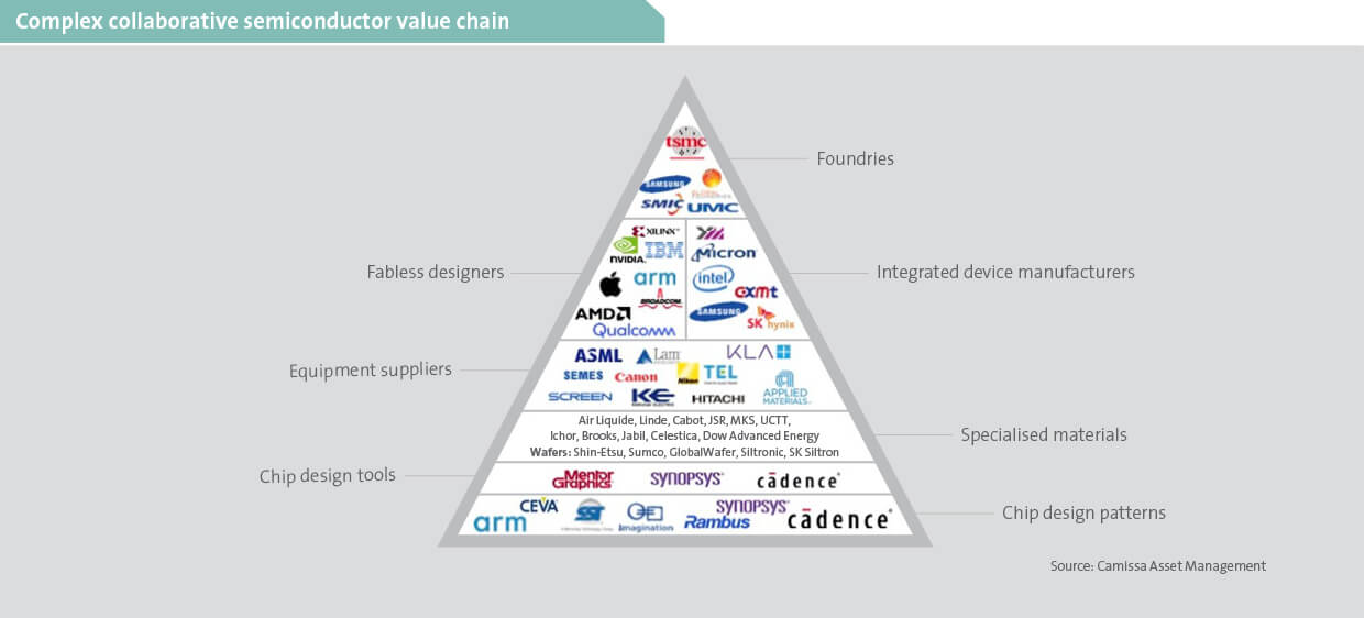
The semiconductor value chain
Modern chipmaking relies on a complex, multiplayer market structure that is highly concentrated and specialised in each stage of the manufacturing process. A handful of companies dominate each segment of the semiconductor supply chain, from fabrication to equipment to materials.
At the front end are chip designers like NVIDIA and AMD who develop the architecture and logic of advanced processors. Semiconductor chips are designed using specialised software provided by companies such as Synopsys and Siemens. Integrated device manufacturers like Intel and Texas Instruments design and manufacture chips, while pure-play foundries like TSMC and GlobalFoundries focus solely on capital intensive, high-volume manufacturing for other firms. Semiconductor testing is dominated by Agilent, Keysight and Advantest.
Applied Materials provides the advanced tools needed to build chips at atomic precision, and companies like ASML lead in critical technologies, for example, lithography. Materials suppliers – another key part of the value chain – deliver vital inputs including silicon wafers, specialty gases and photoresists.
As illustrated below, the entire system depends on deep collaboration and expertise in niche areas, which creates large barriers to entry.
Chipmaking complexity curve
Modern chip design is a complex and capital-intensive endeavour. As feature sizes shrink to just a few nanometres2, the number of steps required to manufacture a single chip has increased considerably. A decade ago, the process may have taken a few hundred separate steps to produce a single chip. Today, advanced chips often require thousands of steps involving complex processes such as deposition, etching, lithography, metrology and others. Furthermore, the number of transistors required for advanced chips can no longer fit into a single die. Chipmakers have therefore begun to build larger and more complex chips to contain multiple advanced processors.
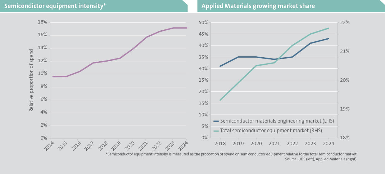
These factors have significantly increased manufacturing complexity, fuelling demand for more advanced equipment capable of finer precision, tighter tolerances and handling exotic materials. Over the last decade alone, semiconductor equipment intensity has grown from just 10% of semiconductor industry revenue to over 17% today (below left).
The power behind the process
Unlike competitors that focus on single product categories, Applied Materials offers a broad and diversified portfolio of tools used across almost every step of the chip production process. Given its strength across several of these steps, it has the unique ability to integrate multiple manufacturing processes into a single vacuum sealed chambered system. These systems minimise contamination, speed up production and, importantly, lead to better chip yields – meaning more usable chips per silicon wafer. For chipmakers, this translates to lower costs and higher process efficiency.
The company’s Applied Global Services division – currently constituting 30% of sales – is also a significant future growth engine. As Applied Materials sells more advanced equipment, the base of machines installed in the field grows. As machines become more complex and harder to maintain and optimise, chipmakers are under greater pressure to establish long-term service contracts with the business. This not only boosts revenue but creates a growing annuity-like income stream.
Applied Materials’ robust intellectual property portfolio – currently comprising over 22 000 active patents – is a major asset. These proprietary technologies position the business strongly in areas like advanced deposition, etching and metrology – all critical to future generations of chips.
Materials engineering is a new frontier
As traditional manufacturing techniques deliver smaller simultaneous gains in semiconductor performance and power consumption, industry focus has shifted to materials engineering – another area where Applied Materials leads globally. Their recent developments around interconnects – the tiny wires that connect billions of transistors within a chip and assist with dissipating heat – highlight the company’s strength in innovation. Today’s most advanced chips can pack more than 90 kilometres of wiring into a space the size of a fingernail. Applied Materials latest solutions have assisted chipmakers to improve performance and energy efficiency by an impressive 25%. It now holds a 41% market share in the engineering materials industry (above right), up from 30% a decade ago. Its market share is generally above 50% across the newer and faster growing areas of demand, supporting an improved growth outlook as these technologies become more widely used.
Attractive financial and R&D model
A unique market position and niche strengths have translated into a strong financial signature for Applied Materials. In the last decade, the company has grown revenues at an average annual rate of 12%, with operating margins averaging a healthy 25%. The business is capital light, yet a significant portion of spend is directed toward research and development (R&D). This high R&D investment (as a proportion of total costs) together with the deep collaboration required between equipment makers and semiconductor manufacturers to tackle complex production challenges, creates substantial barriers to entry against competition.
The model to co-develop tools needed for future production is an underappreciated strength as this allows R&D spend to be targeted toward high growth potential technologies. It also reduces the risk of misdirected capital allocation and enables the company to secure early demand for its products. This collaborative approach has supported a steady rise in returns on capital, which we estimate at over 30%. Moreover, with limited capital needed for growth, incremental returns on capital are high. Over the last decade, Applied Materials has been able to return 90% of cash generated to shareholders through dividends and buybacks.
Positioned for the future
The more complex chipmaking becomes, the more highly specialised the equipment that is required. As a core enabler of cutting-edge semiconductor manufacturing, Applied Materials is strategically positioned to benefit from burgeoning demand. Additionally, it is a clear leader in materials engineering – an increasingly critical frontier in semiconductor manufacturing. With a growing market share in a structurally expanding industry, the growth outlook for the business is very promising.
In addition, Applied Materials’ collaborative R&D model, built on deep relationships with the world’s leading chipmakers, not only seeds future demand but creates large competitive moats. This should sustain a very attractive financial model and future return profile. While the company faces short-term headwinds – including US export restrictions and weaker near-term demand – these pressures have created a rare opportunity to own a global leader, with strong fundamentals at an attractive price.
1The industry term for chip feature size.
2One billionth of a meter, 80 000 times thinner than a human hair.